EE240A : Analog Integrated Circuits
Published in University of California, Berkeley, 2025
I was one of the winners of the Apple Design Competition for this course!
Introduction
This report presents the design of an Operational Amplifier (OpAmp) used as a display driver in a smartwatch application. The subsequent sections encompass the entire design flow - starting from deciding high level design specifications to choice of topology and its reasoning to optimizing the parameters to achieve a high Figure of Merit (FoM) while meeting all specifications.
Figure 1 shows the block level specifications of (a) the display driver and (b) the load model.
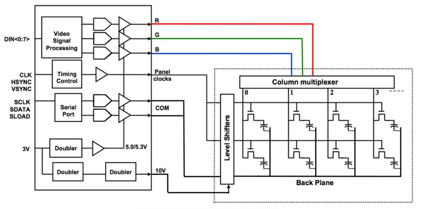
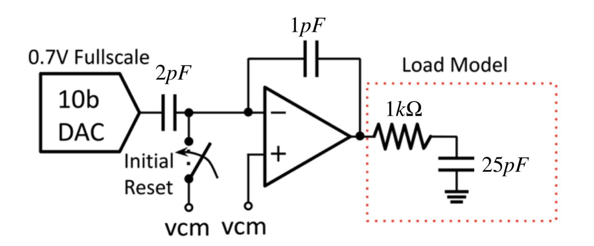
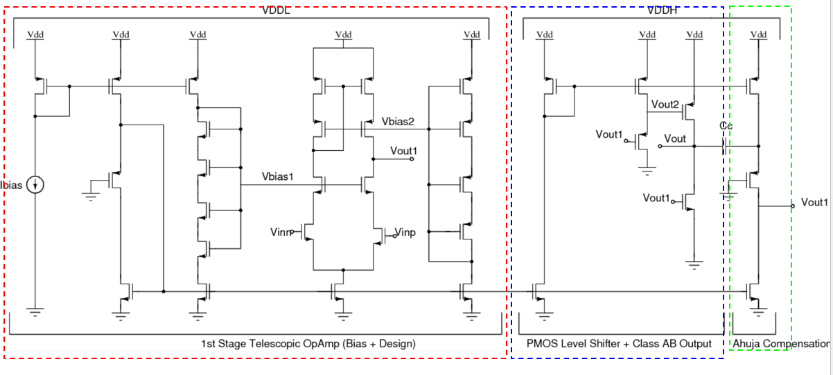
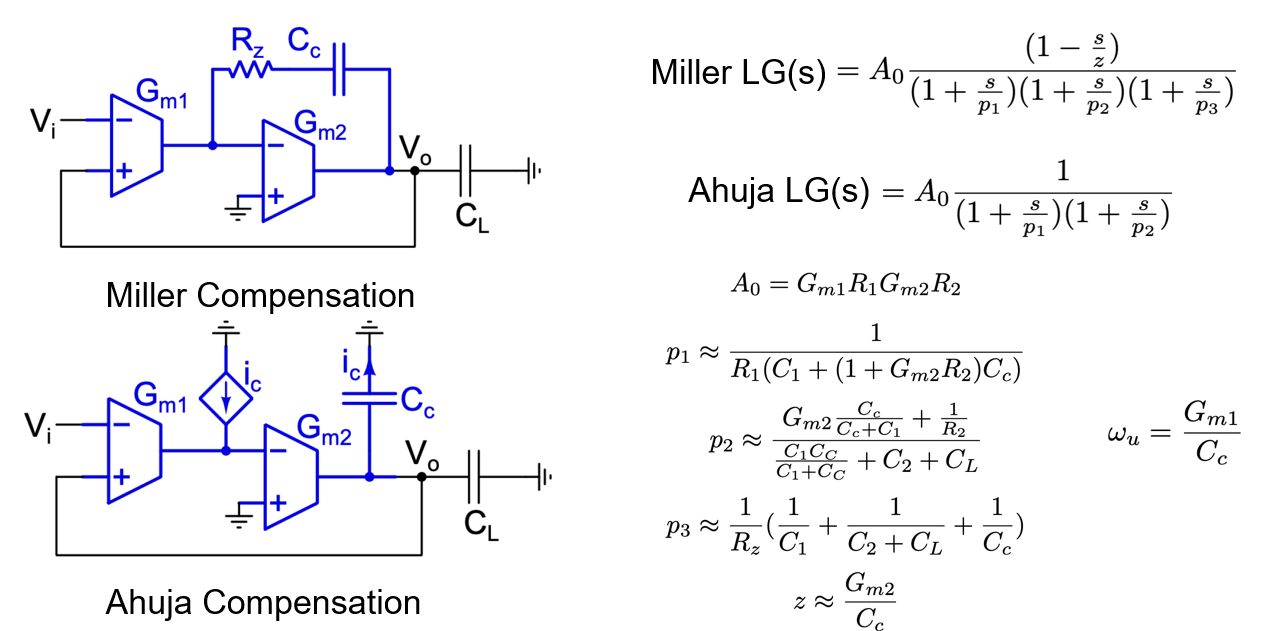
Figure 2 shows the designed two stage operational amplifier. Its highlights are as follows :
- Two Stage Operational Amplifier with Ahuja Compensation
- Telescopic First Stage with 50 dB gain
- Class AB Output Stage with a high slew rate
Translating System Requirements to OpAmp Specifications
An Op-Amp used as a display driver needs to demonstrate a low settling time and a low settling error. Based on the requirement to drive 92480 pixels (obtained by multiplying 272 rows with 340 pixels per row) with a 60 Hz refresh rate, the settling time is computed as
\[T_{\text{set}} = \frac{1}{\text{No. of Pixels} \times \text{Refresh Rate}} = \frac{1}{92480 \times 60} \approx 180 \text{ns}\]The total error provided in the design specification is a sum of the static error and the dynamic error. As a starting point, the total error (\(\epsilon\) = 0.2%) is split equally between the dynamic (\(\epsilon_d\)) and static errors (\(\epsilon_s\)). The dynamic error and the settling time together help us in determining the minimum 3-dB bandwidth of the closed loop required
\[f_{\text{3dB}} = \frac{1}{2\pi} \frac{-\log (\epsilon_d)}{T_{\text{set}}} \approx 6.1 \text{ MHz}\]The static settling error tolerance (\(\epsilon_s\)) provides an estimate of the minimum DC loop gain required for the pixel driver to successfully complete its operation. Since the Op-Amp is used to obtain a closed loop gain of 2, its feedback factor \(\beta = \frac{1}{3}\). This results in a DC loop gain of atleast
\[A_0 = \frac{1}{\beta} (\frac{1}{\epsilon_s} - 1) \approx 3000 = 69.54 \text{ dB}\]Slew rate is often a limitation in driving highly capacitive loads as in this case (= 25 pF).
\[\frac{dV_{out}}{dt} = \frac{V_{\text{out-pp}}}{T_{\text{set}}} = \frac{1.4 V}{180 ns} \approx 7.77 \frac{\text{V}}{\mu\text{s}}\]The above high-level design specifications provide a direction and a set of constraints. These constraints would help us in determining sizes using the gm-ID methodology. However, before we use the script, we need to find out an efficient way to partition the gain requirement and bandwidth requirement across our first and second stages.
Discussion
Topology Choice
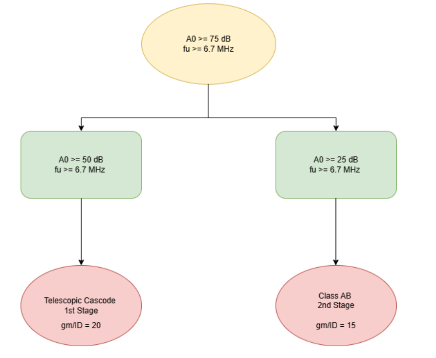
The design uses a two stage topology to meet the high gain specification. The gain (\(\approx\) 75 dB) requirement is split across the two stages in such a way that the bulk of the amplification is done by the first stage (\(\approx\) 50 dB). To achieve this with a high bandwidth, a telescopic cascode is used as the first stage. A class AB output stage is used as the second stage to meet the high output slew rate requirement. Figure 2 shows the schematic of the designed Two Stage Op-Amp. The design was targeted to attain a phase margin of 76\(^\circ\).
For a two pole system, it can be shown that a 76\(^\circ\) phase margin results in a critically damped system resulting in the lowest settling time. In order to achieve the required phase margin, the two stage op-amp was compensated. The compensation technique used draws inspiration from Ahuja Compensation. Instead of the conventional Miller compensation with a resistor Rz, a PMOS transistor is used. It is biased and sized appropriately to achieve a target phase margin of 76\(^\circ\).
Design of the 1st Stage
As reasoned out earlier, a telescopic opamp with a high gain is used as the first stage. The supply voltage of this stage was chosen to be VDDL = 1.1 V to conserve power. All the devices in the first stage were chosen to be nmos2v or pmos2v. On the active load frontier, a high swing cascode was chosen to optimize output swing. The input pair devices, which were constrained to be 2V devices by the problem statement, are operated in sub-threshold region for highest gm-ID (≈ 20) to minimize the first stage bias current. The input common-mode of 500 mV is chosen such that the tail transistor at the edge of saturation. It should be noted that since the second stage is a single ended input and output stage, the burden of meeting the CMRR specification falls upon the first stage. The output DC common mode of the first stage is about 600 mV. While designing with the script, a voltage headroom of Vtail = 100 mV was assumed for the tail current source. A maximum mirroring ratio of 10 is used between any two mirror devices. A PMOS trasistor in Triode is used as a resistor to bias the main mirror that generates the tail bias to conserve on area. By design of the biasing network, all tail transistors are operating with a VDS of \(\Delta V\) at the edge of saturation. This is necessary to ensure that there is no systematic mismatch due to VDS difference across transistors. All devices with total width \(\geq 5\mu m\) are implemented using multiple fingers. The constraints used in the gm-ID script are
\[A_0 \geq 50 \text{ dB}\] \[f_u \geq 6.1 \text{ MHz}\] \[VDD = VDDL = 1.1 V\]Design of the 2nd Stage
A Class-AB Output Stage is used to meet the high slew rate requirement. A PMOS source follower was used as a level shifter to increase the output of the first stage to about 1.2 V. A inverter-style Class AB output stage with its output common mode at mid-rail is designed for optimum swing. The output common mode is sensitive to the common mode of the inputs and has been set by careful tuning of parameters. The supply for this stage is chosen to be VDDH = 1.8 V to meet the output swing requirement. The sizing is done in a manner such that (i) the poles are spaced apart, to meet the target phase margin of about 76\(^\circ\) and (ii) large enough to provide the required current to meet the slew rate requirement. The sizing of the transistor and capacitor for Ahuja compensation was done carefully after the first and second stage were separately tested to meet the performance they individually needed to meet. The gm-ID script was used to optimally size the output stage transistors with a gm-ID of about 15. The following constraints were applied to the gm-ID script while deciding on the initial sizing of the second stage. All devices with total width \(\geq 5\mu m\) are implemented using multiple fingers.
\[A_0 \geq 20 \text{ dB}\] \[f_u \geq 6.1 \text{ MHz}\] \[VDD = VDDH = 1.8 V\]Compensation Choice
In order to achieve a high phase margin as set out earlier, it is necessary to eliminate all unnecessary sources of phase lag. The mathematical argument below justifies why Ahuja serves as a better compensation technique in this case compared to old-school Miller compensation.
As seen from above, Miller compensation results in an additional RHP zero and a pole that causes extra phase lag. Thus, Ahuja compensation proves to be a better option in this case.
Area of the Amplifier
An Apple Watch Series 3 with a 38 mm display (for 272 by 340 pixels) has a display area of 563 mm\(^2\) as specified on Apple’s official specification. The fraction of area occupied by all the amplifiers as a fraction of the total display area is only about 10%.
\[\text{Area of the amplifier= 251.681 } \mu m^2\] \[\text{Total Area of Amplifiers = No. of Pixels} \times 3 \times \text{Area of Amplifier} = 69. 83 \text{ mm}^2\] \[\text{Fraction of Area occupied} = \frac{\text{Area of Amplifier}}{\text{Display Area}} = 12.4 \%\]Results Summary
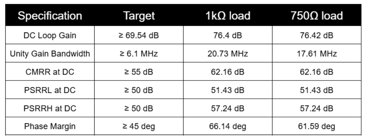
AC Results Summary
Transient Results Summary
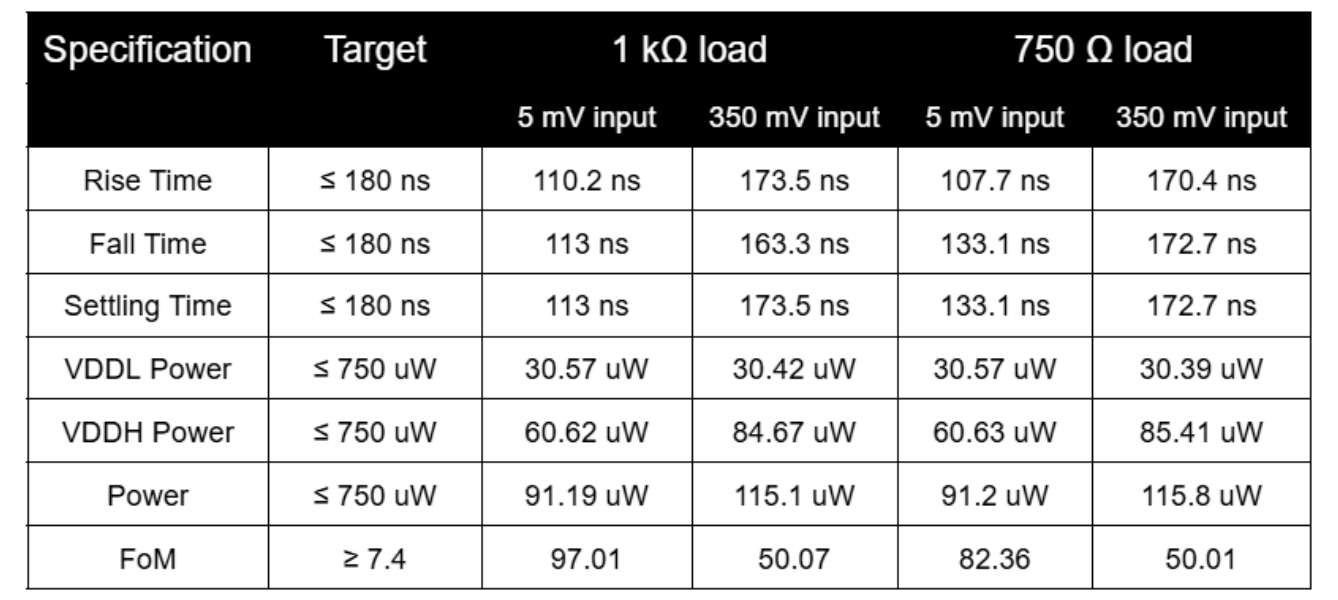
Thus, the designed two-stage OpAmp is able to meet all the required specifications with an overall Figure of Merit (FoM) of 50.01!