EE240B : Advanced Analog Integrated Circuits
Published in University of California, Berkeley, 2026
This project is done in collaboration with Semihcan Seven.
Introduction
The development of high-fidelity neural recording systems is critical for advancing modern biomedical applications, including brain-computer interfaces (BCIs), neuroprosthetics, and continuous physiological monitoring. These systems are tasked with capturing extremely weak biological signals—such as action potentials typically ranging from 0.5 to 5 mVpp — within a low-frequency bandwidth of 300 Hz to 10 kHz. Furthermore, because these recording devices are often integrated into battery-powered, implantable or wearable form factors, their analog front-ends (AFEs) must operate under stringent power dissipation and silicon area constraints.
Designing a robust AFE for neural signal acquisition presents several fundamental challenges. First, the low-frequency nature of the target signals makes them highly susceptible to \(1/f\) (flicker) noise inherent in CMOS transistors, which can easily overwhelm the microvolt-level neural activity. Second, the recording amplifier must exhibit an exceptionally high input impedance (in the tens to hundreds of M\(\Omega\)) to prevent signal attenuation and loading effects at the highly resistive electrode-tissue interface. Finally, maintaining a high dynamic range and low total harmonic distortion (THD) requires a clean, stable supply voltage, necessitating dedicated on-chip power management blocks.
To address these challenges, this report presents the complete system-level and block-level design of a low-noise, high-impedance neural recording signal chain. The proposed architecture features a capacitive-feedback Low Noise Amplifier (LNA) that utilizes a two-stage topology with partial positive feedback to maximize gain and power efficiency. To completely neutralize the \(1/f\) flicker noise within the neural bandwidth, a four-way switch-based chopping stabilization technique is implemented in the signal chain. Additionally, the signal chain includes a custom Bandgap Reference (BGR) and a Low-Dropout Regulator (LDO) to provide robust, isolated power delivery from a 1.1 V battery source.
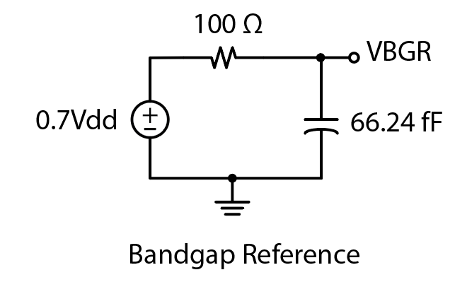
Bandgap Reference Model
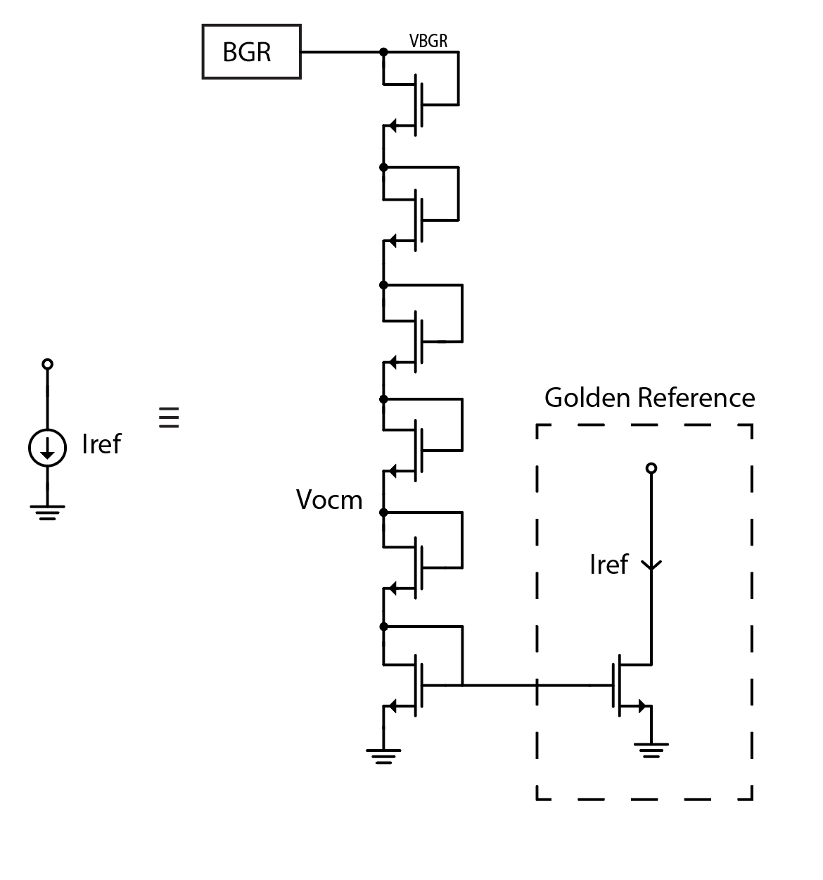
Based on the project specification, our Bandgap reference is implemented as a voltage source of 595 mV with an integrated noise of 250 \(\mu V_{rms}\). To generate the “golden” reference that is used to generate various bias voltages and currents used in other blocks, a pseudo-resistor stack is used to generate a constant set of voltages. The second lowest voltage is set as the output common-mode of the LNA and the lowest voltage is set as the input common-mode of the LNA and is also used to generate the golden current reference of 10 nA for all other blocks.
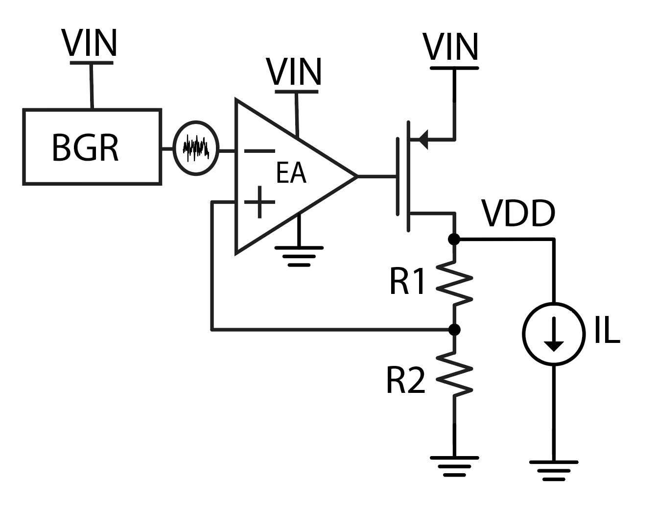
Low Dropout Regulator (LDO)
The figure below shows the capless and resistorless LDO that was implemented. The Error Amplifier (EA) used in the LDO feedback loop is a PMOS-input based folded cascode amplifier as seen on the right in the figure with its biasing details. A PMOS-input based folded cascode amplifier was chosen as the topology of the OpAmp to permit a high input and output common mode range as well as providing very high small signal gain. This opamp was sized using the gm-ID approach.
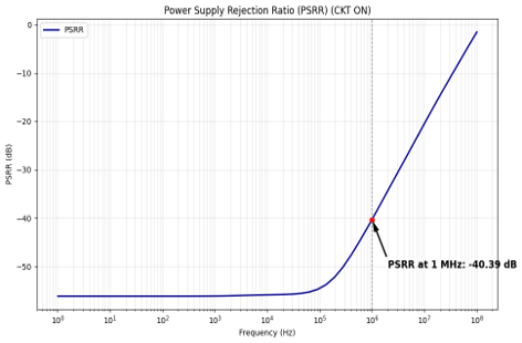
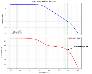
The plots below show the PSRR and Stability of the LDO at the maximum intended current of 10 \(\mu A\). From the transient step responses to a small signal change in supply voltage and reference current, the line and load regulation were calculated to be 9.15 mV/V and 161.48 \(\Omega\) respectively.
Low Noise Amplifier (LNA)
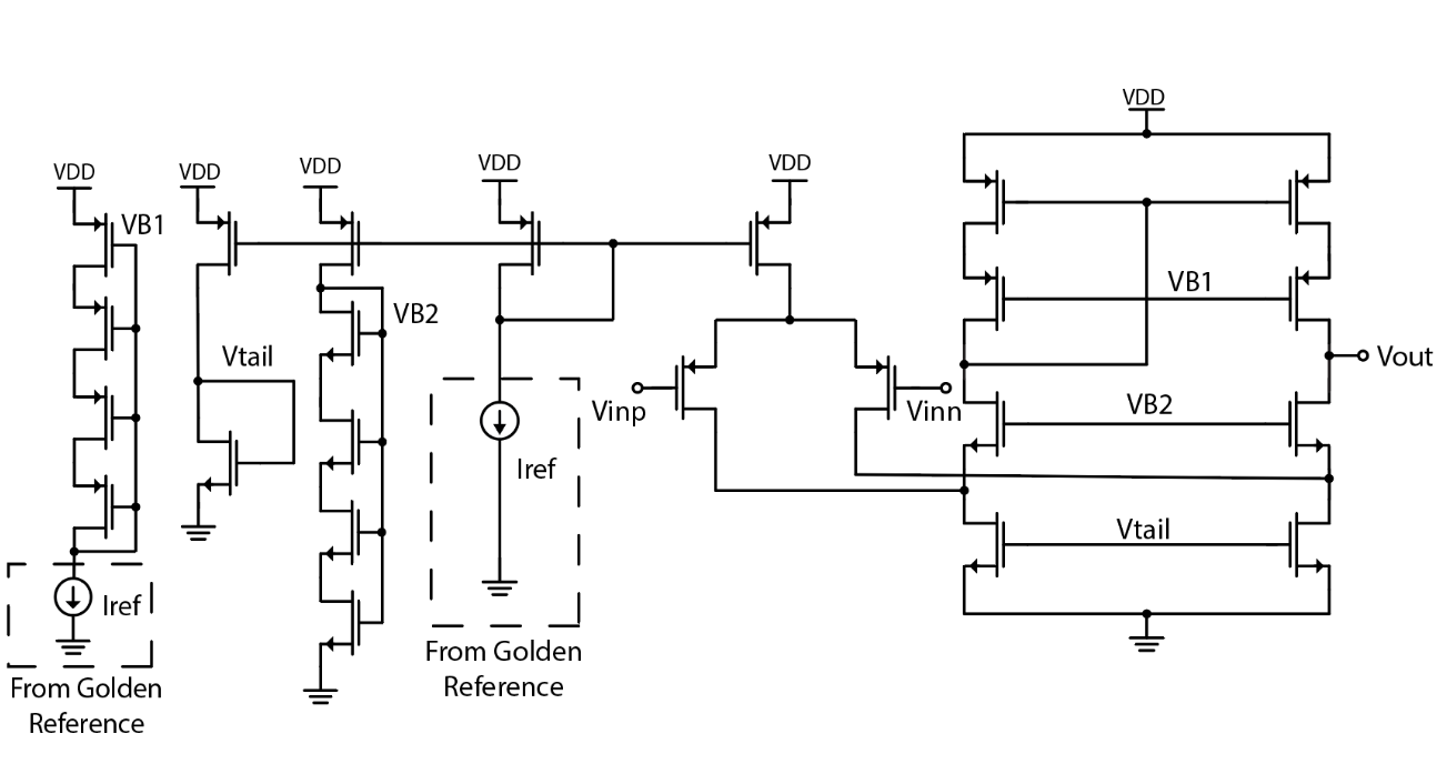
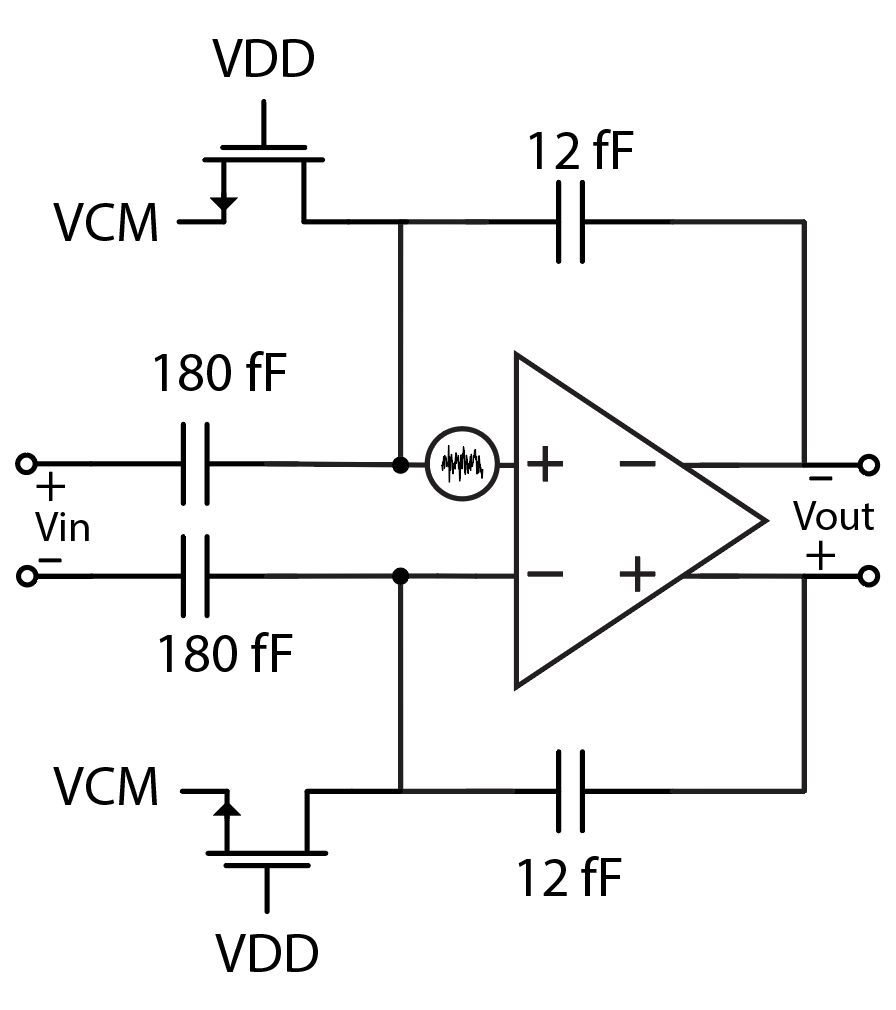
Based on the specifications required to ensure that the input signal at its maximum swing (5 \(\text{mV}_{\text{pp}$}\)) covers the full scale of the ADC when the VGA knob is set to the maximum gain, it can be calculated that the required gain of the LNA is approximately 10. To achieve this gain with sufficient margin, we use a capacitive feedback LNA topology with a closed loop gain of 15. The capacitors are chosen to be 12 fF and 180 fF. These are chosen primarily to ensure that the \(\frac{k_BT}{C}\) noise is minimized while ensuring a low footprint. The area of the LNA is dominated by the capacitors with a footprint of 128 \(\mu m^2\) based on the given capacitor density. The input common mode is set by a large resistor that is implemented as a transistor in triode that places a high-pass corner at around 100 Hz in the closed loop response. Common-mode feedback is done through a simple 5T OTA.
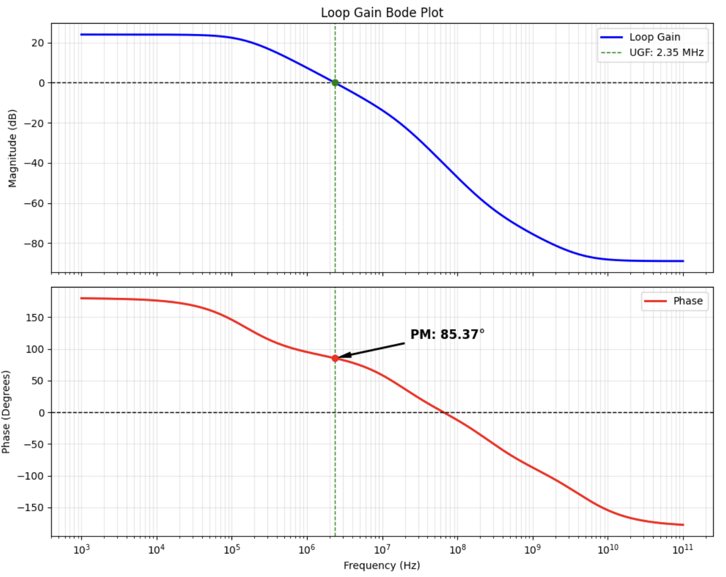
The choice of the amplifier for the LNA is a two-stage amplifier with a partial positive feedback based first stage and a common source amplifier based second stage to achieve a very high gain while ensuring the power dissipation is minimized. While designing, it is ensured that the output impedance seen is always positive across all corners to ensure stability. At the time of design, stability is checked across all possible PVT corners.
System Level Simulations
Though the earlier discussion does not talk about chopping, the actual system level implementation utilizes chopping to ensure that the flicker noise is almost entirely eliminated. Flicker noise is the dominant source of noise in the bandwidth of interest (300 Hz - 10 kHz) and eliminating flicker noise dramatically reduces the noise. Chopping is implemented using the four-way switching topology shown in the figure below.
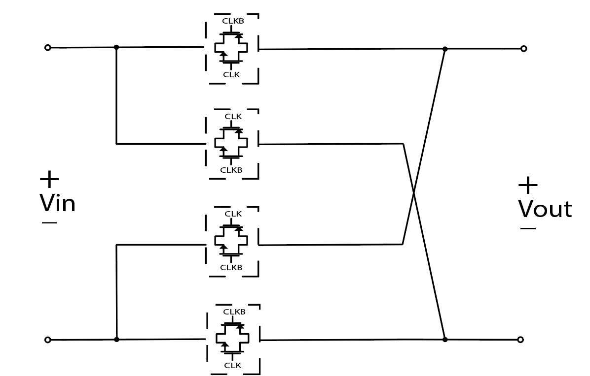
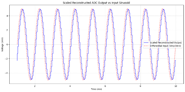
Figure below shows the input differential sinusoidal signal in red and the output of the signal chain after post-processing. It is clearly visible that the input analog signal and the output reconstructed digital data closely follow each other.
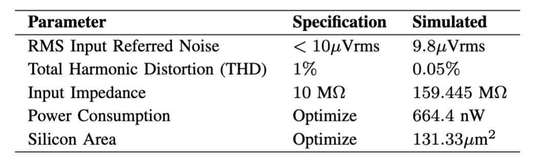
Comprehensive simulation results validate the efficacy of our implementation in TSMCADFP16. The system demonstrates a low input-referred noise of 9.8 \(\mu V_{rms}\), an exceptionally high input impedance of 159.44 M\(\Omega\), and a Total Harmonic Distortion of 0.052\(\%\) at peak input signal swing. Coupled with a measured LDO PSRR of -40.39 dB at 1 MHz ensuring a clean and stable supply, the complete signal chain successfully satisfies all target specifications, proving its viability for high-fidelity, continuous neural action potential acquisition in power-constrained environments. The overall system level results are summarized below.
Our design achieves a Figure of Merit (FoM) of 11460.57!