EECS251LB : Field Programmable Gate Array Laboratory
Published in University of California, Berkeley, 2025
This project is done in collaboration with Somil Jethra. We won the Apple Design Competition for this Design!
Introduction
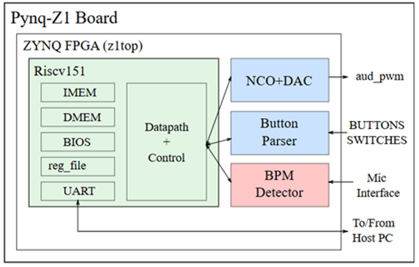
This project implements a 32-bit RISC-V core with a 3-stage pipeline, synchronous instruction/data memories, with minimal stalling and an integer cycles per instruction of 1. In addition to integer operations, the processor also supports floating point operations with a floating point CPI of slightly greater than 1. UART is used to interface the core with the real world. This RISC-V core was fully implemented on a PYNQ-Z1 board as shown in Figure 1.

3 Stage Pipeline
The three stage pipeline is divided into three phases :
- F : Instruction Fetch
- DX : Decode and Execute
- MW : Memory and Write-Back
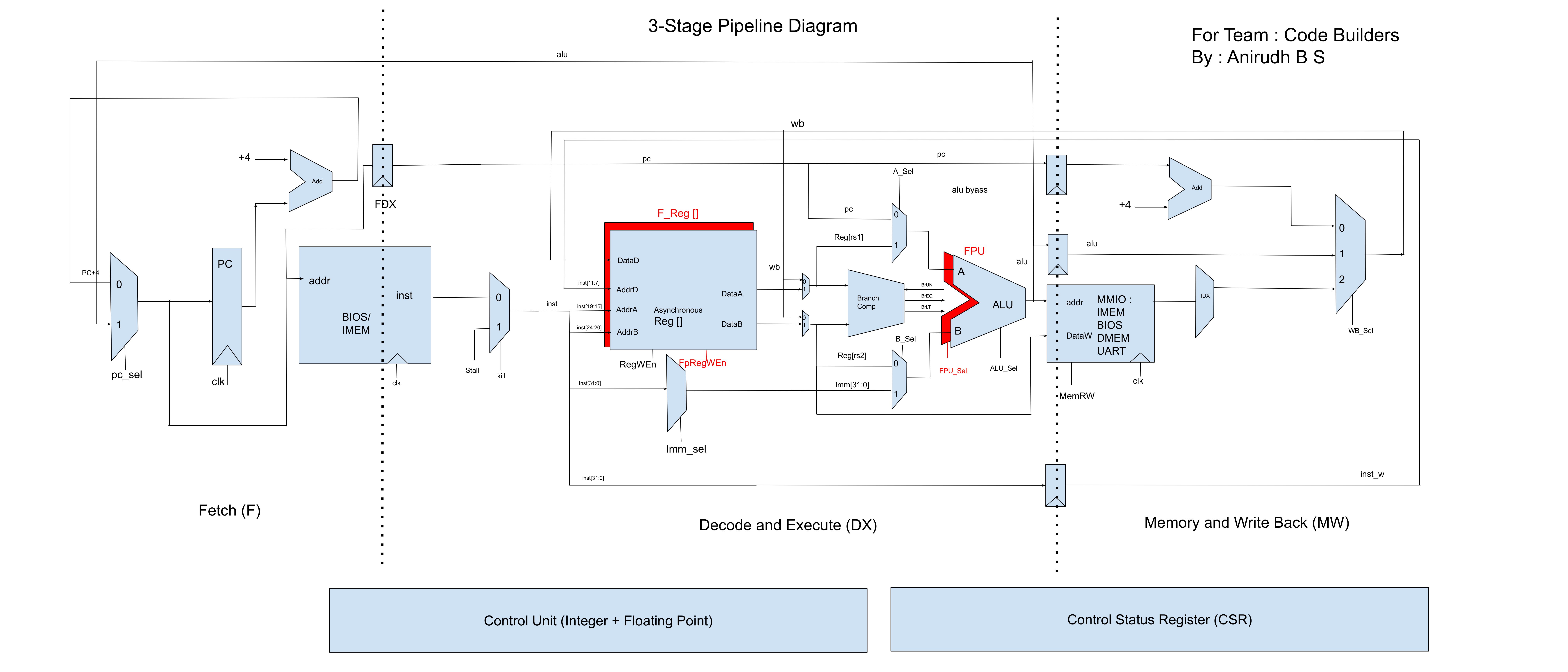
Figure 2 shows the Block Diagram of our three stage pipeline with Floating Point Unit in parallel to the ALU. The Floating Point Unit (FPU) is pipelined with 2 stages for floating point addition and 3 stages for floating point multiplication and accumulation.

In the F stage, the IMEM, PC and pipeline register are clocked simultaneously. Between the DX and MW stage, the DMEM and pipeline registers are clocked together. Extensive forwarding is employed to ensure that ALU-ALU hazards, MEM-MEM hazards, MEM-ALU hazards and ALU-MEM hazards do not encounter any stalls. The PC Select Mux takes one of its input right from the output of the ALU. In case of a branch instruction, the ALU output is directly forwarded to the IMEM address, thus reducing any branch misprediction and having a resultant integer CPI of 1.
Due to the long critical path of the floating point unit, it has been pipelined to 2 stages for floating point addition and 3 stages for floating point multiplication and accumulation to ensure high frequency of operation.
Memory Mapped IO
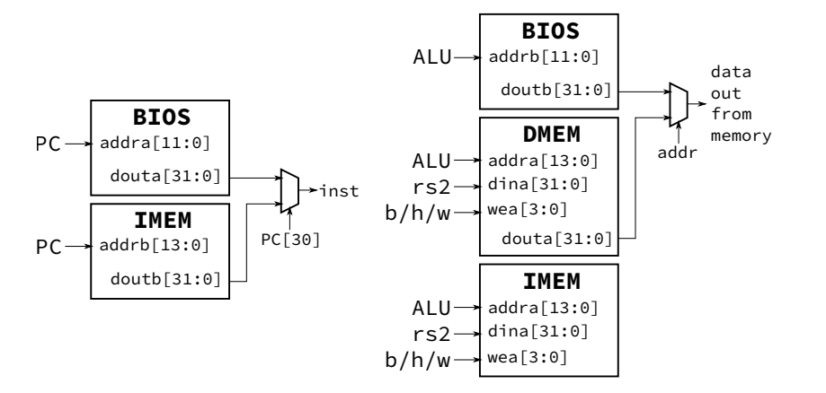
A memory mapped IO is used to map the different memory locations to IMEM, BIOS, DMEM and UART modules. Figure 3 shows the MMIO mapping of the RISC-V core.

Resource Utilization
FPGA Usage
| FPGA Resource | No. of Units |
|---|---|
| LUTs | 2589 |
| SLICE registers | 567 |
| BRAMs | 34 |
| DSP Blocks | 2 |
Critical Path
The timing of the critical path is 15.744 ns.
Results
| Parameter | Value |
|---|---|
| Integer CPI (mmult) | 1 |
| Integer CPI (bdd) | 1 |
| Floating Point CPI (fpmmult) | 1.33 |
| Clock Frequency | 62 MHz |
| Cost | 4138844 |
| Figure of Merit (FoM) | 22.96 |
The achieved Figure of Merit (FoM) is 22.96!