EECS251B : Advanced Digital Integrated Circuits
Published in University of California, Berkeley, 2026
This project is done in collaboration with Semihcan Seven.
We won the Apple Design Competition for this course!
Introduction
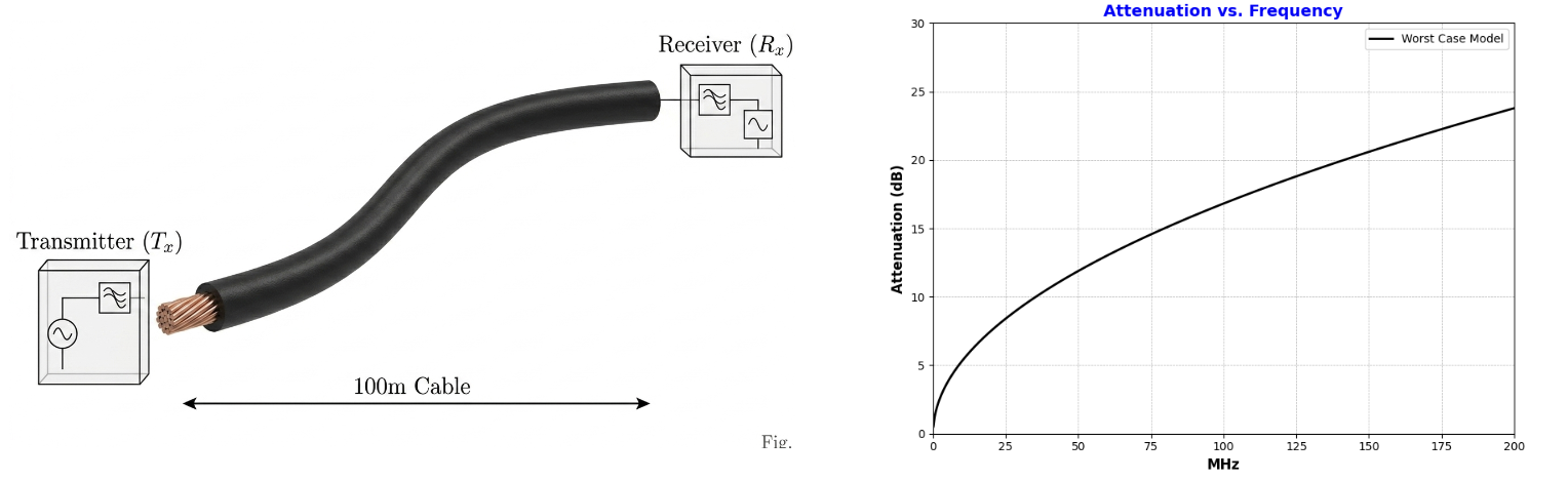
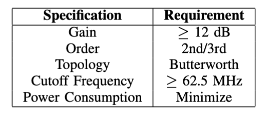
This project talks about the design of an Analog to Digital Converter (ADC) and its Anti-Aliasing Filter (AAF) for Gigabit Ethernet (GbPHY) applications. The Analog to Digital Converter (ADC) is arguably the most critical and power-hungry block in the Gigabit Ethernet (GbPHY) receiver chain. The burden of amplifying the low swing analog signal received from the channel and quantizing the resulting signal into digital values that can be recognized by the backend digital signal processing. At 125 MHz, the channel loss is estimated to be about 20 dB. The anti-aliasing filter upfront is tasked with restoring the incoming analog signal to the ADC full scale. This is in addition to the original function of removing aliasing components.
Flash ADCs are extremely fast at the expense of high power and large silicon footprint. Oversampling or Noise-Shaping ADCs provide extremely good SNR but need signficantly higher sampling rates and in 130 nm, these do not seem feasible. Successive Approximation Register (SAR) ADCs often are implemented using time-interleaving and are sensitive to the settling of the DAC output. Pipelined ADCs provide a right balance between all of the important metrics - speed, throughput, power and area and thus, our design uses a pipelined ADC.
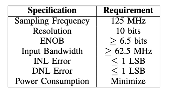
Tables 1 and 2 summarize the required specifications for both the Anti-Aliasing Filter and the ADC based on the requirements outlined in the IEEE Gigabit Ethernet standardization requirement.
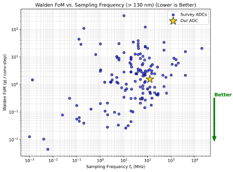
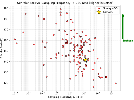
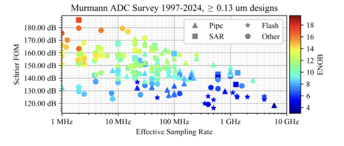
The figure below shows the distribution of ADCs across various topologies implemented in 130 nm and older technologies. The survey was done by Boris Murmann and can be found on his website.
Anti-Aliasing Filter (AAF) Design
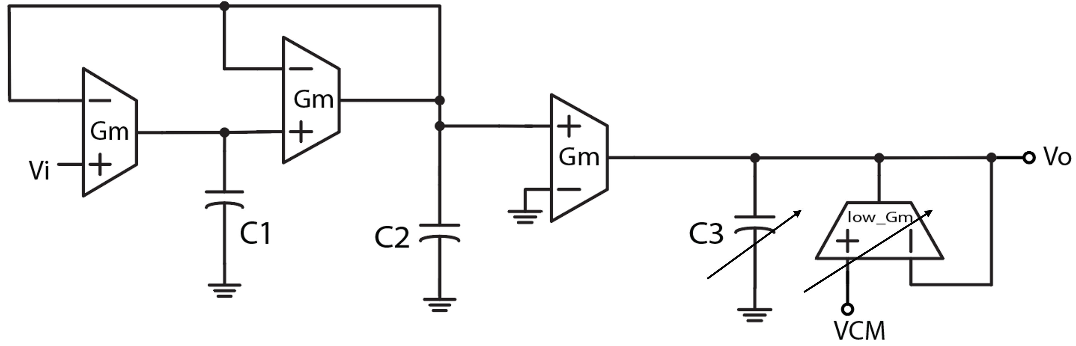
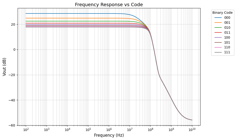
The Anti-Aliasing Filter forms the heart of the analog front end. The Anti-Aliaisng Filter amplifies the incoming analog signal such that the incoming signal matches the full scale range of the ADC for maximum resolution. The Anti-Aliasing Filter (AAF) is responsible to ensure that the input to the ADC is not aliased. Literature survey suggests the use of an active gm-C filter or a Biquad filter. However, the design of a Tow-Thomas Filter requires the OpAmps used in the Biquad filter to have a very low output impedance. This automatically results in an excessively large power being dissipated in the output stage to obtain a very low output impedance. To circumvent this problem, we adopted a gm-C filter that can easily be tuned by changing the capacitor values and tuning the bias current to change the current. The figure below shows the schematic of the implemented AAF. The actual implementation is pseudo-differential since the ADC is fully differential.
For some tunability, the bias current of the low gm resistor and capacitor are left tunable to account for variations of input signal level and process variations. The figure below shows the results of the layout extracted filter.
Analog to Digital Converter (ADC) Design
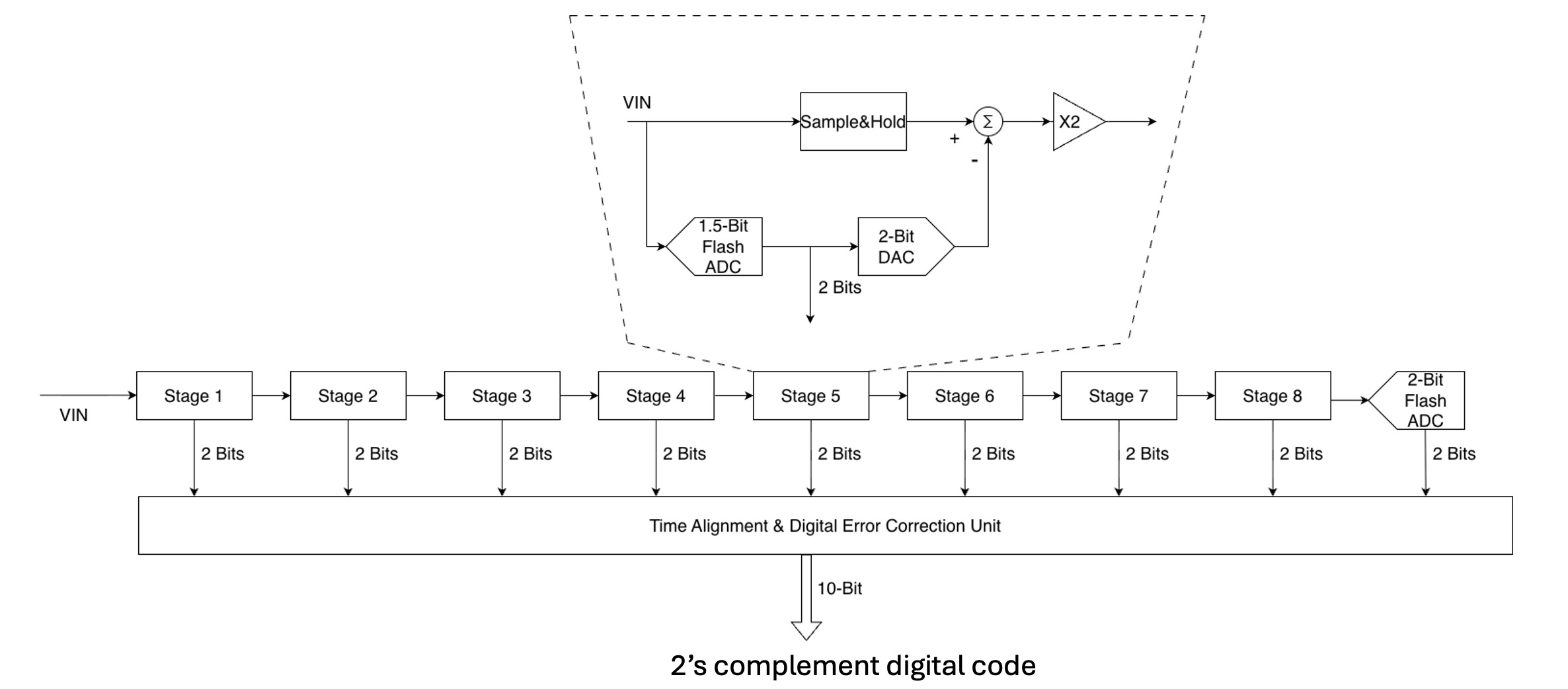
The block level diagram of the pipelined ADC is shown below.
The MDAC forms the most critical analog block in the pipeline stage. The implementation uses a fully differential switched-capacitor topology centered around a high-bandwidth operational transconductance amplifier (OTA). The design of this amplifier is described later in the next subsection. During the sampling phase \(\phi_1\), the analog input is captured across a parallel array of sampling capacitors. The sampling phase is followed by a comparator phase during which the sub-ADC use the sampled values to make a decision on the binary value that is used in the amplification phase that follows and the overall digital backend. During the amplification phase, the feedback network is reconfigured on the basis of the digital decisions provided by the Sub-ADC. The capacitors are selectively connected to the positive or negative reference voltages to perform Sub-DAC subtraction. The ratio of the input capacitors to the feedback capacitor is sized to provide the required gain of 2. Because the OTA must settle to within a fraction of a Least Significant Bit (LSB) within half a clock cycle (approximately 4 ns at 125 MSPS), a high-gain and high-bandwidth OTA is needed. The figure below shows the schematic of the MDAC.
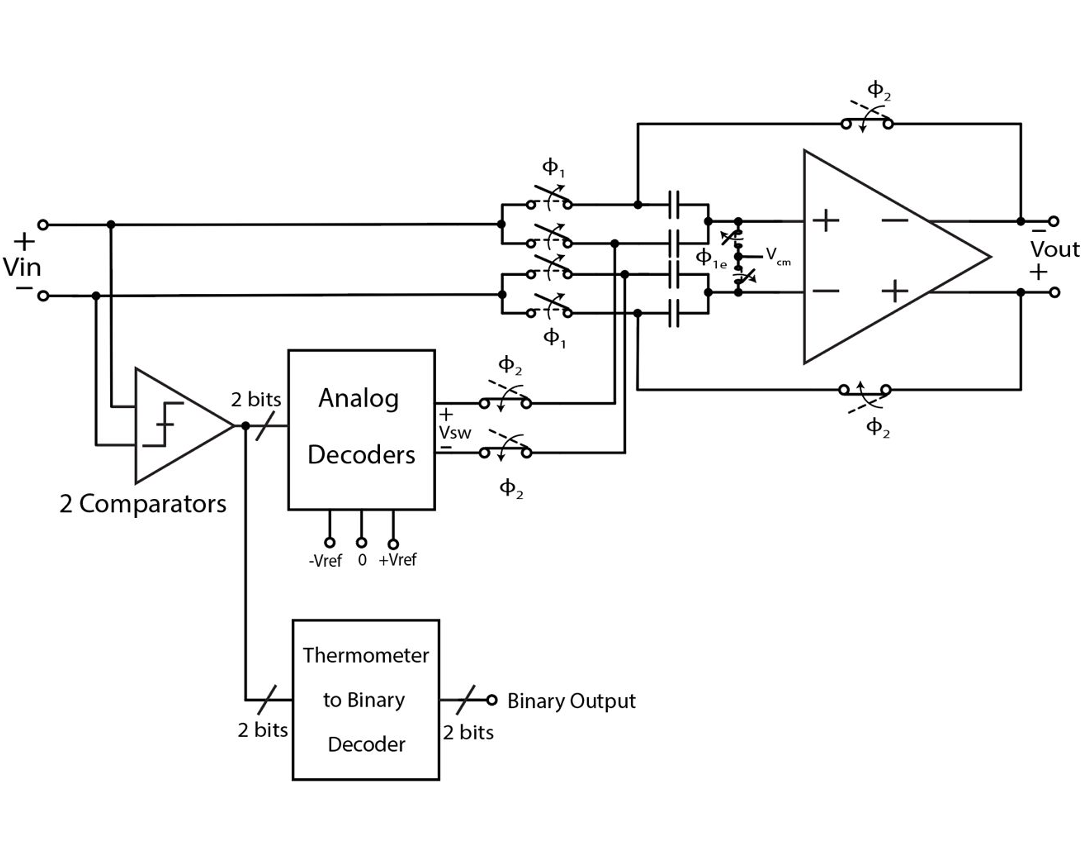
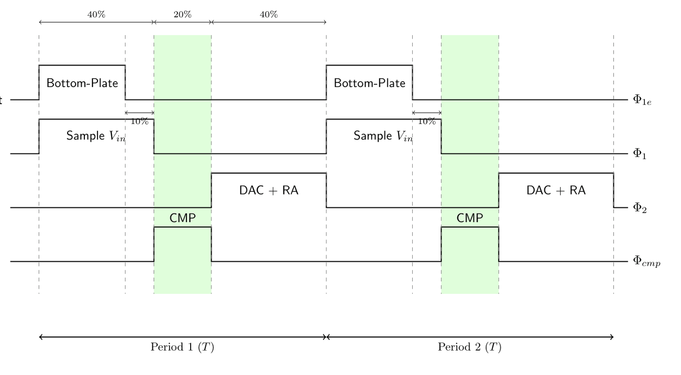
Figure below shows the timing waveforms required to implement the MDAC successfully.
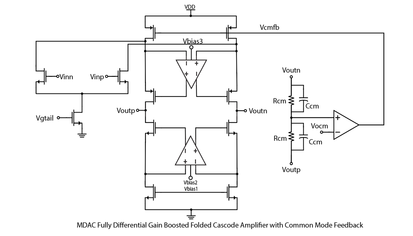
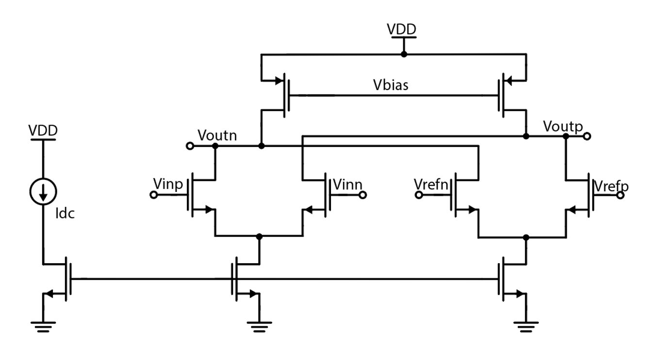
To obtain a very high gain, it is necessary to use a cascode topology or a two stage implementation. The gain requirement of the OpAmp is set to be 72 dB based on the 0.5 LSB required resolution. The need for a very high bandwidth necessitates the use of a single stage; thus, we adopted a fully differential gain-boosted folded cascode amplifier with common-mode feedback. Figure below shows the schematic of the op-amp. The common mode-feedback amplifier is a simple 5-transistor amplifier. gm-ID technique was used to optimize the sizing of the transistors for maximum gain while minimizing power consumption.
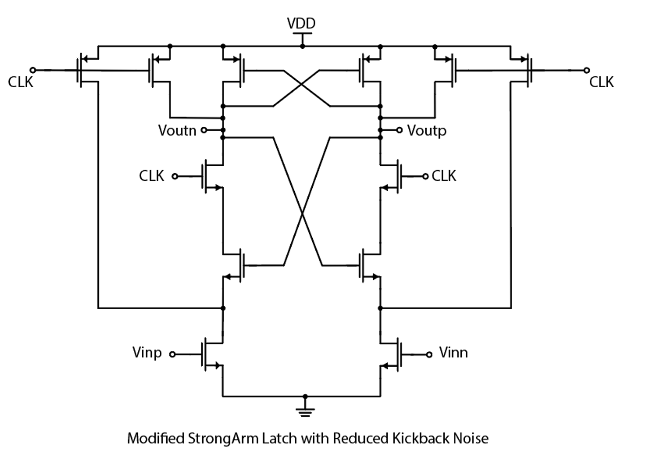
The figures below describe the design of the comparator. The conventional Strong-Arm Latch has two phases - the precharge phase and the regenerate phase. During the precharge phase the outputs are shorted to VDD. During the regeneration phase, the comparator makes a decision on the voltages that need to be compared. Compared to the conventional topology shown on the left in the figure below, the topology on the right has a lower kickback noise and thus, have adopted that topology in our design. However, the reduced kickback noise comes at the cost of a higher offset that needs to be compensated by adding a pre-amplifier before the strong-arm latch.
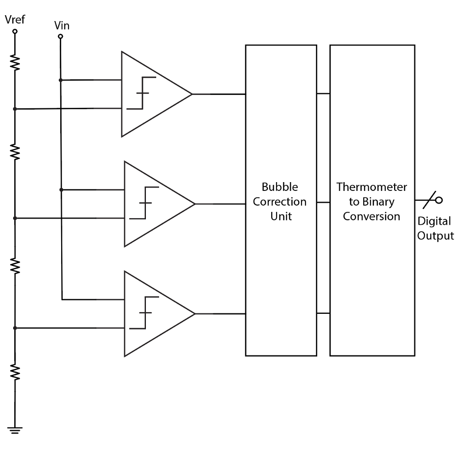
The block diagram of a 2-bit flash ADC is shown below. The coarse quantization within each stage is performed by a 1.5-bit Flash sub-ADC that utilizes two comparators. This block utilizes a resistive reference ladder to generate threshold voltages. Because the architecture employs a sub-radix gain of 2, rather than the ideal gain of 4 for a 2-bit stage, structural redundancy is introduced into the quantization process. This redundancy significantly relaxes the offset constraints on the comparators. Small threshold errors caused by process variations or device mismatches will not saturate subsequent pipeline stages. Each stage includes a bubble correction logic to combat glitches and also a thermometer to binary decoder to get the final binary digital output.
Simulation Results
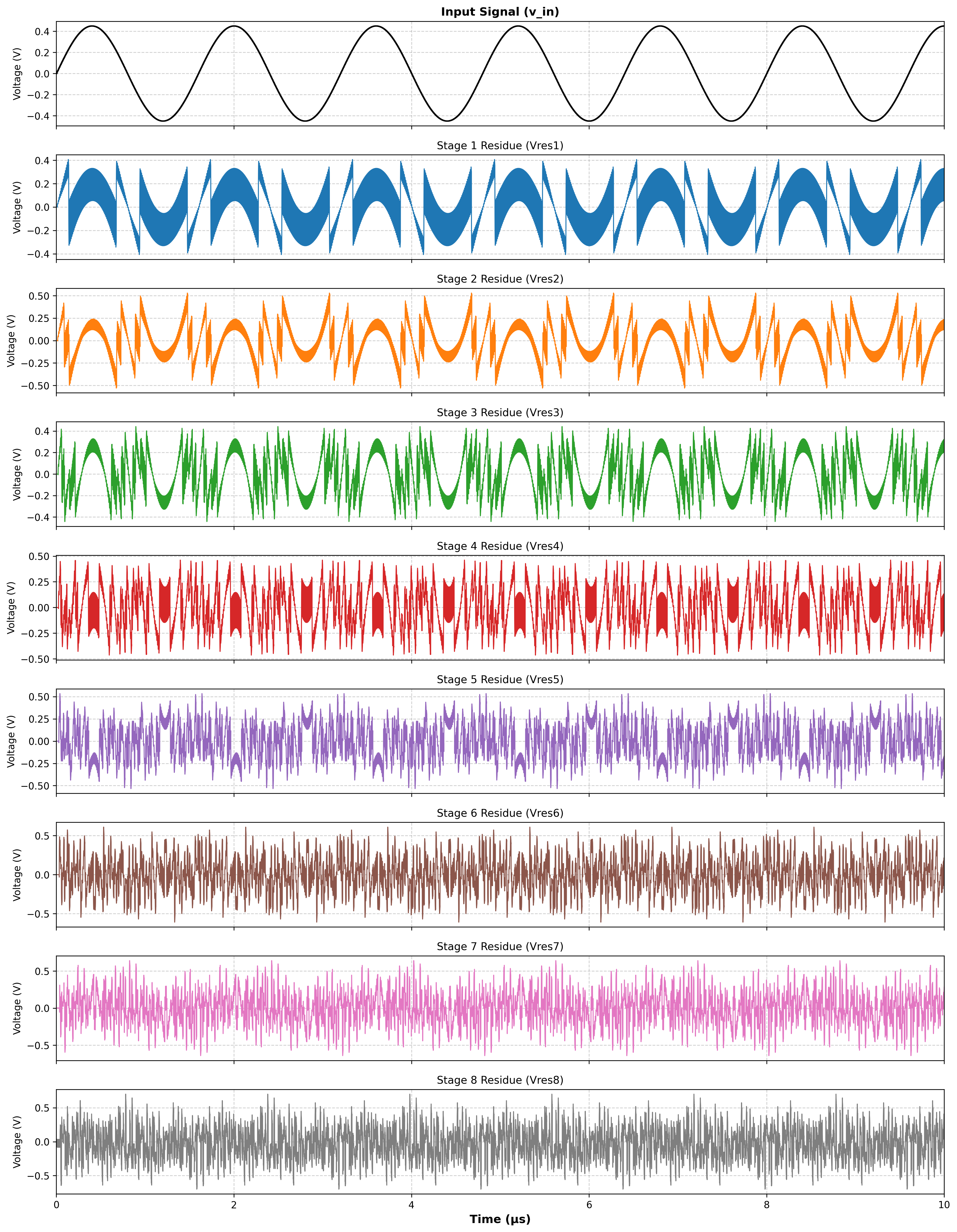
The residues across each stage is shown in the figure below.
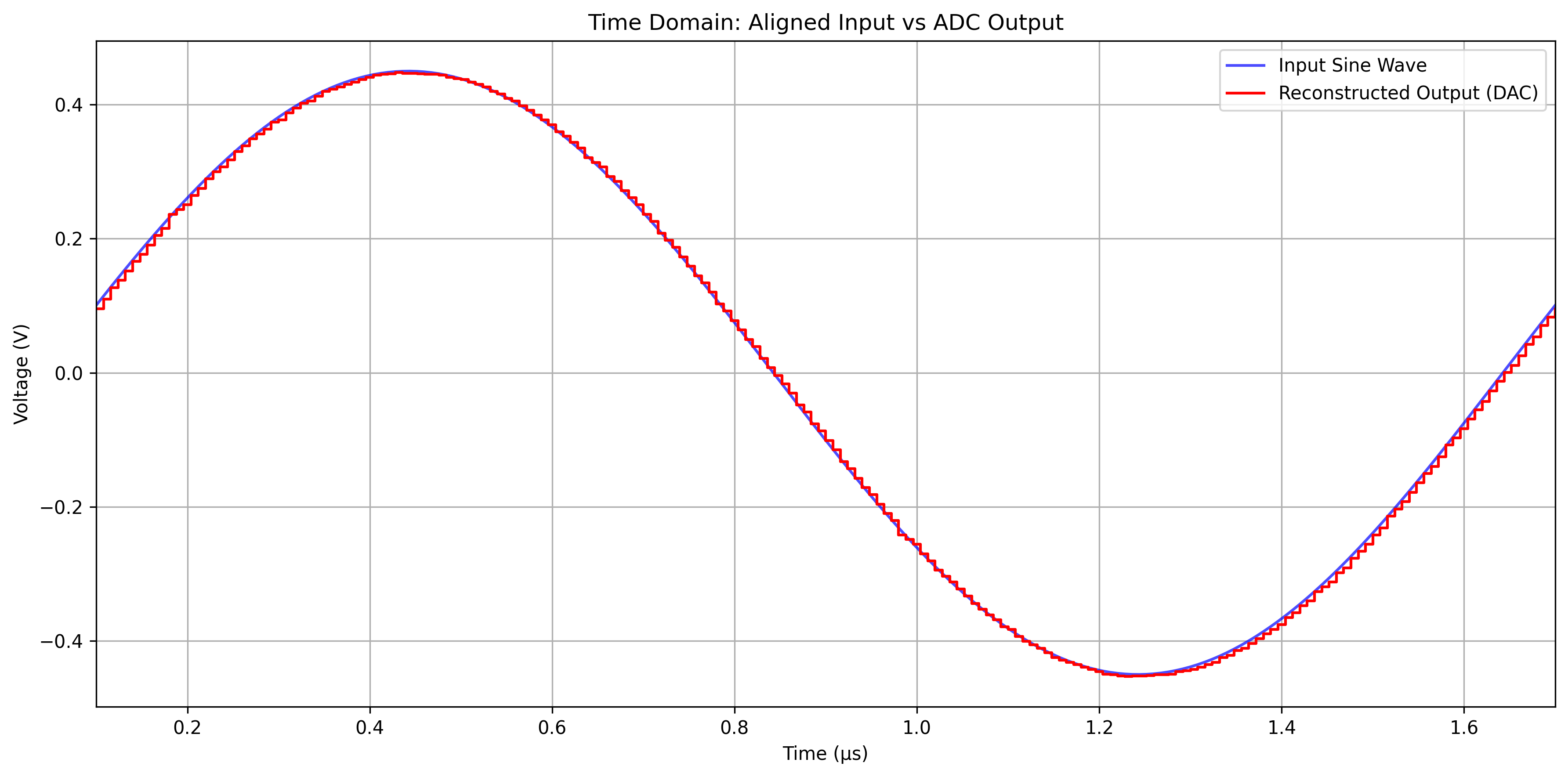
Figures below show the input sinusoid versus reconstructed ADC output and the Output Spectrum respectively.
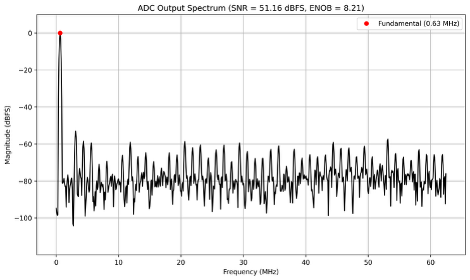
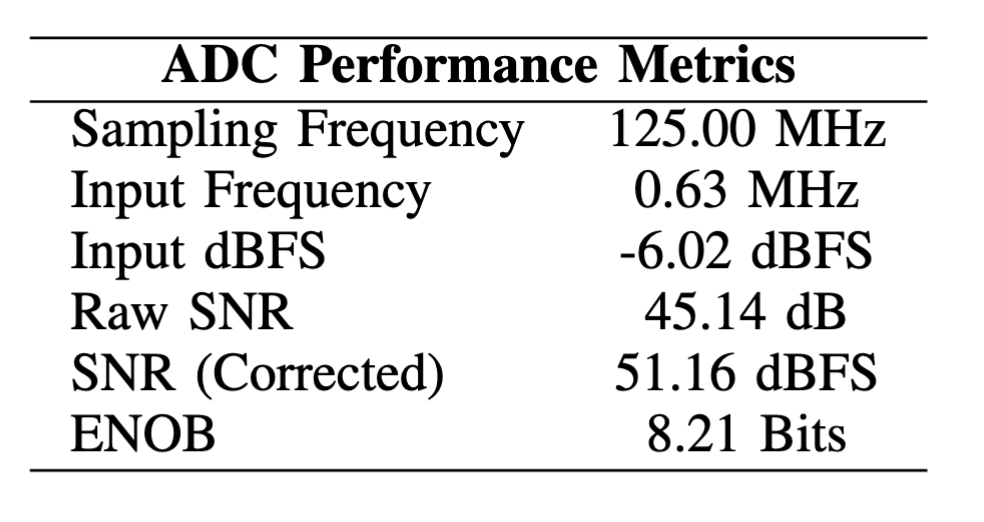
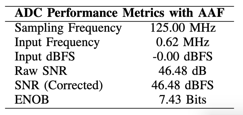
The tables below show the simulation results of the ADC and integrated AAF + ADC respectively. The attained ENOB is 8.21 and is comparable to state of the art ADCs at ISSCC.
Figures below show the Walden and Schreier FoM of our ADCs with ADCs published at ISSCC. The performance of our ADC is at par with state of the art ADCs published at ISSCC.